All conductors always have resistance, inductance and capacitance. As a circuit designer it is important to know how large these so-called parasitics are and when they are significant.
In general parasitics become more important with increasing frequency.
All parasitics end up being proportional to length therefore as a general rule conductors should be kept as short as possible. This typically means that wires and cables are the first to show parasitics.
Contents
Parasitics
Resistance
Resistance is the most familiar non-ideality of components. It is related to material conductivity (copper vs aluminum etc.) and cross-sectional area.
There are tables commonly available that provide resistance in Ohms/meter of all wire gauges.
Circuit boards also have resistance, where you need to consider trace width and layer thickness for the cross-sectional area.
Less frequently discussed are the AC effects on resistance. The first is skin effect, where current remains near the surface (i.e. skin) of conductors. The second is proximity effect, which is similar to skin effect but induced by currents in adjacent conductors. The latter is typically considered in inductor and transformer design.
Contact resistance can be another factor. Any two conductors in physical contact have a non-zero contact resistance at their interface depending on the contact surface areas, material type/finish, cleanliness and contact pressure. Contact resistance is typically highly variable and hard to predict.
Inductance
Inductance is the component of impedance that increases with frequency. This means that it first appears as a signifcant parasitic in low-impedance circuits such as power lines and high-speed data lines.
Inductance is a result of magnetic field and therefore depedent on the loop area of the current path. The key to reducing inductance is to keep the line and return as close together as possible.
Fast changing or high currents are most affected by inductance because:
\(v_L = L \frac{di}{dt}\)
Capacitance
Capacitance is the component of impedance that decreases with frequency. Therefore it first appears as significant in high impedance circuits such as operational amplifier circuits and CMOS logic.
Capacitance is associated with electric fields and therefore depedent on conductor surface areas and proximity. The key to reducing capacitance is to keep conductors small and far away from eachother.
Fast changing or high voltages are most affected by capacitance because:
\(i_C = C \frac{dv}{dt}\)
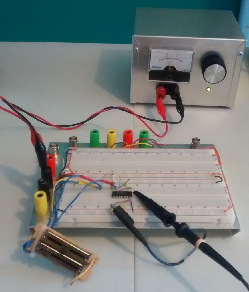
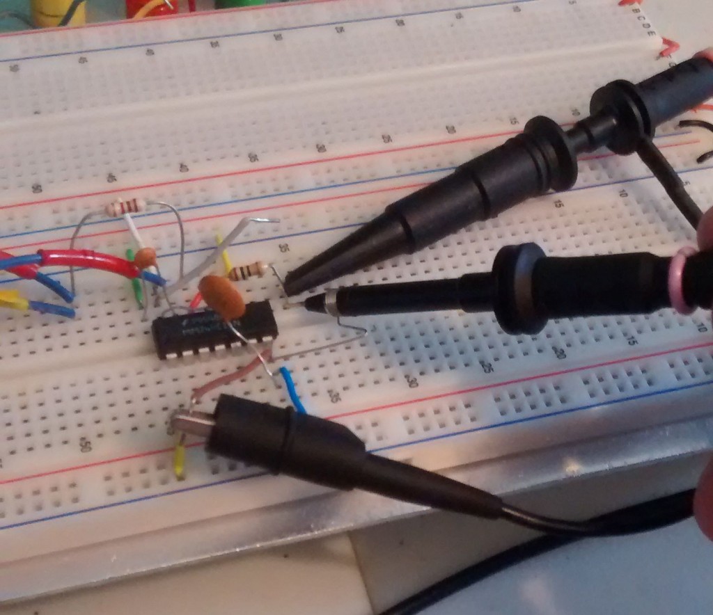
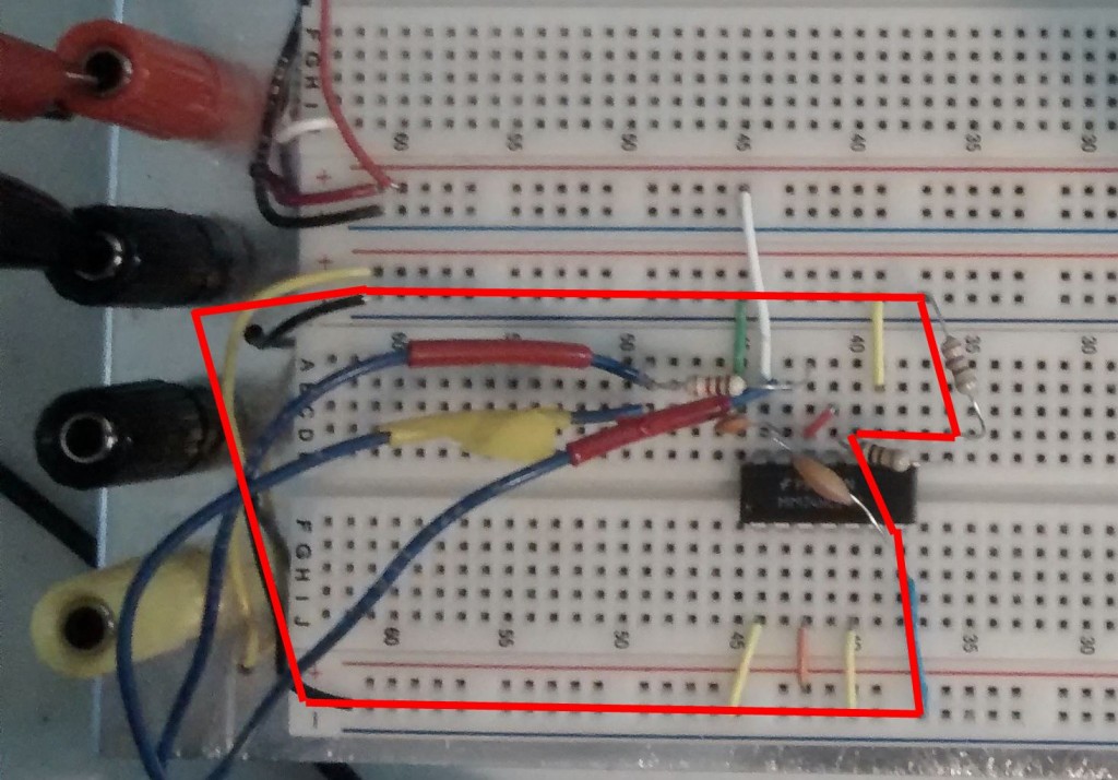
Example: Solderless Breadboard
A solderless breadboard is a typical prototyping tool especially for students and hobbyists. It is also notoriously affected by parasitics.
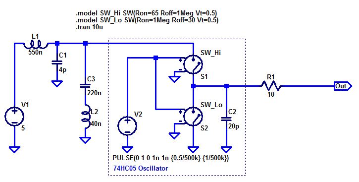
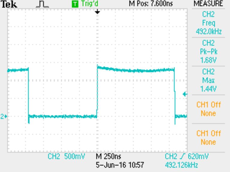
The test circuit is a 5V CMOS oscillator operating at between 50 kHz and 500 kHz, based on a potentiometer setting. The input power is 5V coming through a pair of twisted alligator clip probes about 30 cm long. The IC is from the “HC” logic family with a rise time of approximately 3 ns.
Initial Measurements
The idealized circuit model and the test setup are both shown below.
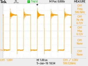
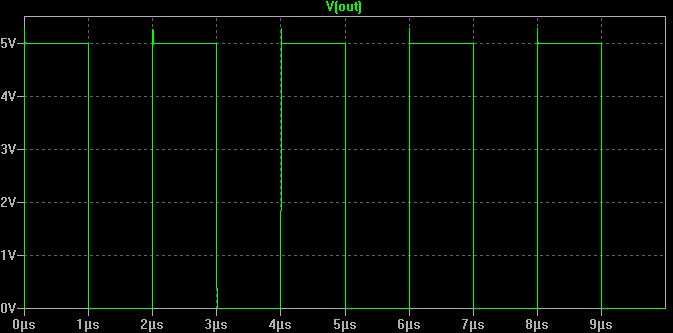
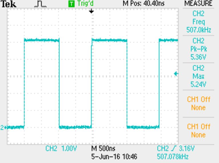
These are the measured waveforms for both 50 kHz and 500 kHz operation:
50 kHz – measured peak overshoot is 6.0 V (20%).
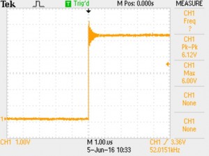
500 kHz – measured peak overshoot is 6.1 V (22%).
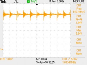
Clearly the overshoot is not very strongly related to the frequency, and the two plots look almost identical on the edges — this overshoot and ringing is due to the fast edge, not the repetition frequency.
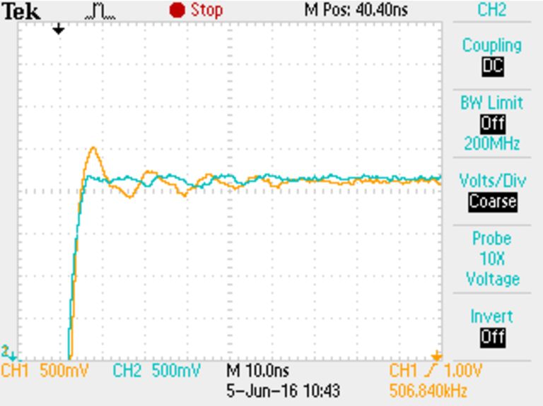
This is the 5 V voltage rail – showing 5.8 V peak ripple.
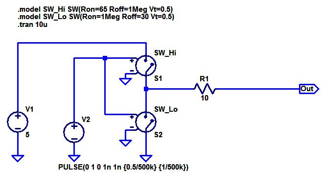
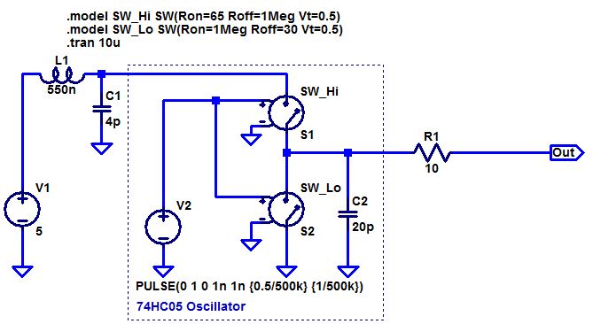
Adding the Parasitics to the Model
The cause of all this ringing is of course parasitics. First, there is a large amount of inductance in series with the power line.
The alligator clips are something like 1 uH/m, so 300 nH total for 30 cm. The breadboard power and ground strips are about 8 cm long from the banana posts, and the spacing between them is 5 cm. This is approximately 250 nH using the inductance of a square loop formula (assuming 6.5 cm average side length). Wiring is approximately 10 pF/m, so there is about 4 pF of capacitance in the wiring and breadboard.
In the existing model there is actually no load current, because the output is open-circuit. We can estimate the internal IC power consumption as a capacitance at the switching node.
We can add these elements to the circuit model:
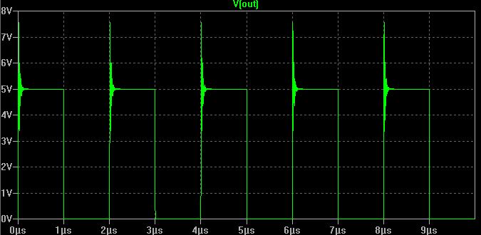
This plot looks a lot more realistic.
Adding a Decoupling Capacitor
We can reduce this problem by adding a decoupling capacitor directly to the IC power pins. For this test a 220 nF capacitor was added, which with it’s approximately 3 cm of lead length has an inductance of about 40 nH. The simulation shows a great improvement:
Probe Parasitics
There is still another major source of error in this setup — the probe itself. The probe ground is attached to the circuit using a long alligator clip, which forms a loop about 5 cm x 5 cm, or about 200 nH. This is in series with the probe resistance (10 Megohm) and capacitor (~12 pF).
A better alternative is to use a ground spring tip, shown below.
And here is the scope plot of the two probes at the same time, zoomed in on the overshoot. The ground clip adds an extra 10% overshoot to the measurement in this case.
After adding the decoupling capacitor and using the better probe termination, the circuit looks as good as the simulation.
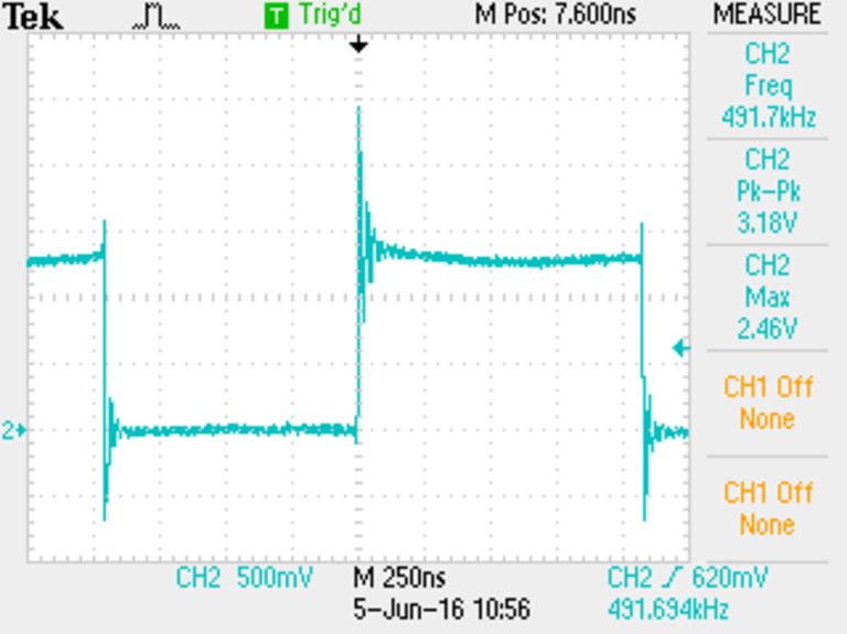
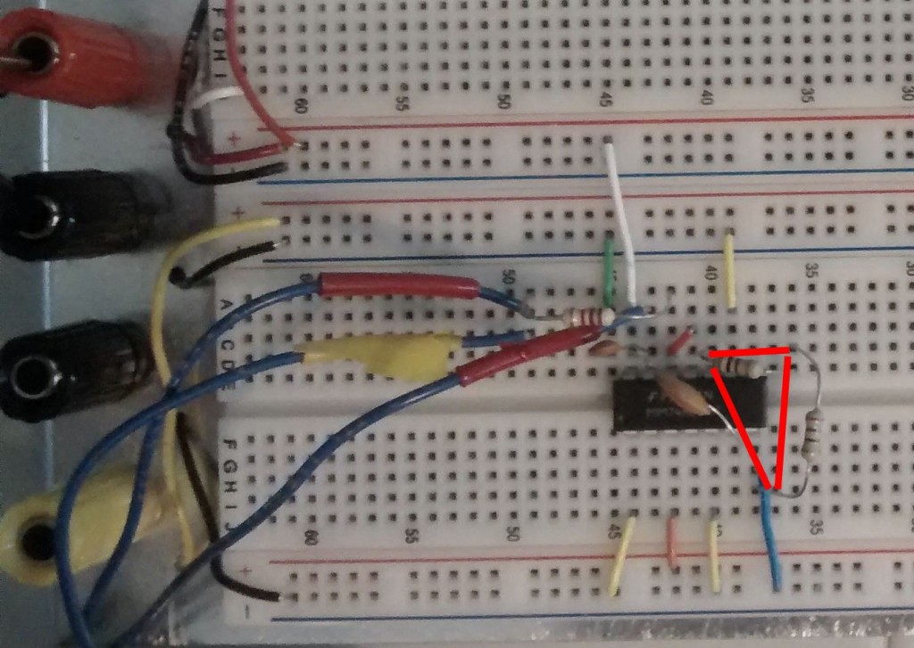
Load Return Path
The previous measurements were without a load. Now, we add a 27 ohm resistor which draws significant current from this logic output.
If we don’t pay attention to the path of current we can accidentally introduce serious inductance.
The first location will have the resistor go from the output to the top ground rail, while the IC is connected to the bottom one. You can see the large current loop traced out in red, and the resulting terrible ringing on the output. The inductance of this loop is approximately 250 nH.
Note that the low voltage of the waveform and is due to the low resistance load, which is less than the output resistance of the oscillator.
Now we take the same load and move it directly to the IC return pin, and see the situation improved dramatically.
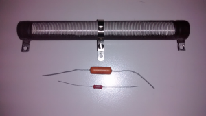
Example: Wirewound Resistors
Many power resistors are constructed by winding a coil of wire around a ceramic substrate.
A typically wound resistor coil is definitely also an air-core inductor, though non-inductively wound resistors also exist.
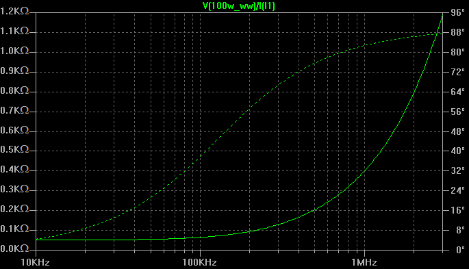
As a comparison, three resistors were measured for inductance:
100W, 51 ohm, wirewound resistor (length = 165 mm) : 63 uH
5W, 0.5 ohm, wirewound resistor (length = 20 mm) : 0.13 uH
0.5W, 6.8 ohm, film resistor (length = 9 mm) : < 0.1 uH
The net result (shown below) is that at 1 MHz, the 100W resistor is actually 396 ohms with 82 degrees phase!
The 5W resistor fares a lot better, being only 0.96 ohms at 58 degrees phase.